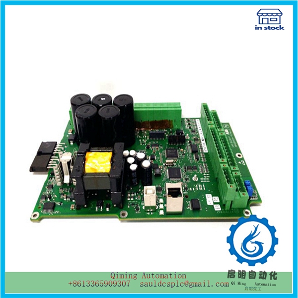
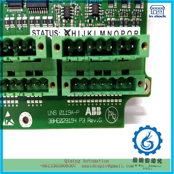
UNS0119A-P 3BHE029153R0101 3BHE029154P3 | ABB | Response to main device module
¥8,288.00
Module Number: UNS0119A-P 3BHE029153R0101 3BHE029154P3
Product status: Discontinued
Delivery time: In stock
Sales country: All over the world
Product situation: Brandnew , one year warranty
Contact me: Sauldcsplc@gmail.com +8613822101417 SIMON
Have a good day! Thanks for watching my website!
Introduced Product:
PM866K01 3BSE050198R1
9907-1200
MAX-4/11/03/128/08/1/1/00
8200-1300
UAD149A0011
VE3007 K2005X1-BA1 12P4375X012
C400/A8/1/1/1/10
IS220PVIBH1A
3500/65 145988-02
KUC755AE106 3BHB005243R0106
Description
UNS0119A-P 3BHE029153R0101 3BHE029154P3 | ABB | Response to main device module
- .Many products are not yet on the shelves please contact us for more products
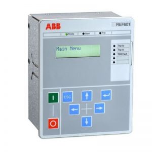
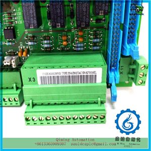
- .If there is any inconsistency between the product model and the picture on display, the model shall prevail. Contact us for the specific product picture, and we will arrange to take photos in the warehouse for confirmation
- .We have 16 shared warehouses around the world, so please understand that it can sometimes take several hours to accurately return to you. Of course, we will respond to your concerns as soon as possible
UNS0119A-P is a clock, while SDA carries data. When SDA changes from 1 to 0 and SCL remains 1, it indicates the start of data transmission. The next 7 digits are the address of the device. Next is the read and write flag, which is read when it is 1 and write when it is 0. If there is a device on the I2C bus that corresponds to the requested address, the slave device will send an ACK signal to notify the master device that data can be sent. After receiving the ACK signal, the main device sends an 8-bit data. After the transmission is completed, SCL remains at 1, and when SDA changes from 0 to 1, it indicates the end of the transmission.
From this timing chart, it can be seen that SCL is very important, and which clock edge is for what is determined. For example, the first 7 must be addresses, the 8th is a read/write flag, data transmission must be 8 bits, an ACK signal must be received, and so on
UNS0119A-P requires a master device responsible for initiating requests and controlling the clock; Other devices are slave devices that identify and respond to master device requests through device ID addresses. The master and slave devices need to take turns controlling SDA. At first, I didn’t understand this point, so I added I2C data code and measured it using an oscilloscope at the SDA and UNS0119A-P pins. However, I could only find some messy waveforms without the expected effect. Later, the slave device was connected, and the code was written on both sides, responding to each other. Only then did the waveform be seen on the oscilloscope.
Mailbox:sauldcsplc@gmail.com |UNS0119A-P 3BHE029153R0101 3BHE029154P3
www.abbgedcs.com | Qiming Industrial Control | Simon +86 13822101417
We may provide the information of this product:
Guidance manual PDF /Datasheet/ Weight/ Size/ Orignal country/ Prodcuct COO & COM & COC
Certificate of conformity / Certificate of Origin / Certificate of Origin /Operation method
Delivery time/ Provide a one-year warranty / Brand New Original Authentic

Reviews
There are no reviews yet.